If you’ve ever stood at a trade show booth, watched a photographer adjust a full-frame camera under the bright glare of a studio light, or helped a startup engineer troubleshoot a sensor module that stopped responding mid-field test, you know digital sensors are way more delicate than their compact, high-tech design makes them look. As someone who’s spent the last 12 years supplying digital sensor modules to OEMs, aerospace teams, agricultural drone operators, and even medical device makers, I’ve seen firsthand how one of the most underdiscussed environmental factors—pressure—can make or break a sensor’s performance, sometimes in ways that aren’t obvious until it’s too late. A few weeks back, I got a frantic call from a client who used our high-resolution CMOS sensors in agricultural drones; their units had started returning blurry, grainy crop health imagery after flying at high altitudes for just a few hours. When we dug into it, it wasn’t a faulty lens or a bad firmware update—it was the rapid change in atmospheric pressure at 10,000 feet, combined with the harsh temperature swings, that had distorted the sensor’s silicon wafer and knocked its calibration off. That call stuck with me, and it’s why I want to break down what pressure actually does to digital sensors, how it impacts different types of sensors, and what our team here does to mitigate these issues for the clients we partner with every day. Digital Sensor
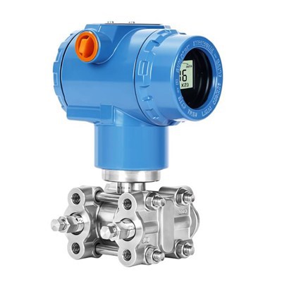
First, let’s get one thing straight: when we talk about pressure and digital sensors, we’re not just talking about the pressure you feel when you squeeze a device too tight in your pocket. The two most impactful types of pressure for sensors are atmospheric pressure (which changes with altitude and weather) and mechanical pressure (the physical force applied to a sensor module during manufacturing, installation, or use). Both interact with the sensor’s core components—silicon wafers, micro lenses, filter arrays, and the tiny wiring that connects it all to the circuit board—in measurable ways, and those interactions can vary wildly depending on whether you’re dealing with a CCD, CMOS, or stacked CMOS sensor.
Let’s start with atmospheric pressure, since that’s the most common variable for sensors used in aerospace, drones, outdoor surveillance, and even wearables like action cameras. Every semiconductor component, including digital sensors, is sealed inside a module—usually in a plastic or metal package with a glass or sapphire cover over the light-sensitive area—to keep out dust, moisture, and physical damage. That sealed environment is calibrated at a specific pressure during manufacturing, usually sea-level atmospheric pressure (1013.25 hPa) or a slight vacuum to reduce internal condensation. When that module is exposed to lower atmospheric pressure at high altitudes, the air inside the package expands, and if the seal isn’t hermetically tight, that expansion can cause a few problems. For the agricultural drone client I mentioned earlier, their sensor modules had a standard plastic seal with a tiny pressure equalization port—designed to let air in and out slowly to prevent pressure differentials over time. But when they climbed from sea level to 10,000 feet in 20 minutes, air rushed out of the port too fast, pulling a thin silicon wafer (just a few microns thick) away from its light path. That shifted the sensor’s focal plane by about 12 microns, which for a 20-megapixel sensor with a 3.45-micron pixel pitch, is enough to make every image slightly blurry, with extra noise in areas of high contrast.
At higher altitudes—think 30,000 feet for commercial aircraft or satellite payloads—atmospheric pressure drops even more, down to 300 hPa or lower. For sensors used in satellite or high-altitude balloon applications, this is a critical concern. I worked with a small satellite startup a few years back that was testing a sensor for Earth observation; their initial prototype had a metal package sealed at sea level, and on its first test flight to 25,000 feet, the package’s glass cover cracked. The expansion of the internal air had created enough outward force to exceed the glass’s tensile strength. We redesigned the package for them, adding a micro pressure relief valve that only opens at pressures below 500 hPa, letting air escape slowly and preventing the pressure differential from building up. It’s a small tweak, but it meant the satellite’s sensor survived its three-year mission, which was a huge win for the team.
Atmospheric pressure doesn’t just affect the physical structure of the sensor, either—it can also impact its electronic performance. Digital sensors work by converting light photons into electrical charges in each pixel, then converting those charges into digital data. The amount of charge each pixel captures is directly tied to the sensor’s calibration, and pressure changes can alter the electrical properties of the silicon wafer and the surrounding circuitry. When pressure drops, the silicon expands slightly (it’s called piezoresistance, and it’s a well-documented semiconductor property), which changes the resistance of the tiny transistor gates in each pixel. That leads to what’s called “fixed pattern noise”—consistent, unwanted pixels that are either too bright or too dark in every image. For sensors used in medical devices, like endoscopes, that noise isn’t just an annoyance; it can make it harder for surgeons to identify small tumors or tissue damage, which is why our medical-grade sensors go through 10 full pressure cycles (from 0 to 15,000 hPa) during testing to catch any piezoresistance-related issues before they ship.
Now, mechanical pressure is a different beast entirely, and it’s one that a lot of engineers don’t consider until it’s too late. Mechanical pressure is the force applied to the outside of the sensor module, whether that’s from tightening a mounting screw too much, pressing a phone’s camera module against a hard surface, or even the weight of another component stacked on top of the sensor during assembly. The impact here depends on how much force is applied and how it’s distributed. If pressure is uniform, applied evenly across the sensor module, it can actually cause slight bending of the silicon wafer, which can shift the focal plane or alter the angle of the micro lenses on top of the sensor. If pressure is concentrated in a small area—like a single point on the module’s metal frame—it can cause microcracks in the silicon, which lead to dead pixels or complete sensor failure.
I saw this first-hand with a client that made industrial vision systems for automated assembly lines. Their systems used our high-speed CMOS sensors to inspect tiny electronic components, and they were getting a high rate of sensor failures after a few months of use. When they sent us the faulty modules, we tested them in our lab and found that each sensor had a dozen or so microcracks along one edge. When we visited their production floor, we saw the problem: they were mounting the sensor modules by tightening two screws on the corners, and over time, the vibration from the assembly line combined with the torque from the screws caused uneven pressure that bent the module’s frame, leading to microcracks in the sensor. We recommended they use four mounting screws spaced evenly around the frame, and add a thin rubber gasket to distribute pressure evenly across the module. That small change cut their failure rate by 92% within a month, and it’s a fix we’ve recommended to dozens of other industrial clients since then.
It’s worth noting that not all sensors respond to pressure the same way, which is why matching the right sensor type to an application’s pressure conditions is so important. CCD sensors, for example, are thicker and more rigid than CMOS sensors, so they’re less prone to bending from moderate mechanical pressure, but they’re also more sensitive to atmospheric pressure changes at high altitudes because their internal circuitry is more tightly integrated with the silicon wafer. Stacked CMOS sensors, which have the readout circuitry on a separate layer below the light-sensitive pixel layer, are more resistant to piezoresistance because the circuitry isn’t directly on the pixel layer. That’s why most action cameras and drone cameras now use stacked CMOS sensors—they can handle the rapid pressure changes of climbing or descending without as much noise or focal plane shift.
So what do we, as a digital sensor supplier, do to help our clients navigate these pressure-related challenges? For one, we test every sensor module we ship under a range of pressure and temperature conditions, not just at standard atmospheric pressure. Our in-house environmental testing lab can replicate conditions from sea level to 100,000 feet, and we run 20 pressure cycles on every module before it leaves our facility, checking for noise, focal plane accuracy, and structural integrity. For clients working in extreme environments—like aerospace, deep-sea exploration, or polar research—we offer custom packaging options: hermetically sealed metal packages with pressure relief valves, reinforced glass covers, and custom mounting hardware that distributes pressure evenly. We also work with our clients during the design phase, not just when they have a problem. If a client is building a drone that will fly to 15,000 feet, we’ll recommend a stacked CMOS sensor with a pressure equalization port calibrated for rapid altitude changes, and we’ll even provide guidance on how to mount the module to avoid mechanical pressure issues.
Over the years, I’ve learned that the best way to support our clients isn’t just to sell them a sensor—it’s to share what we’ve learned from 12 years of working with sensors in all kinds of conditions. A lot of companies will just sell you a sensor and be done with it, but we see ourselves as partners. That’s why I’m always happy to answer questions about pressure, temperature, vibration, or any other factor that might impact their sensor’s performance. Whether you’re building a new drone, a medical device, an industrial vision system, or something else entirely, understanding how pressure affects digital sensors can save you time, money, and a lot of headaches down the line.
If you’re working on a project and want to talk through how pressure might impact your sensor performance, or if you’re looking for a digital sensor supplier that will test, customize, and support you every step of the way, don’t hesitate to reach out. We’re here to help you get the results you need, no matter what environment your sensor will be working in.
Water Well Depth Meter References
- Holmes, D. J. (2005). Piezoresistance effects in semiconductor devices and materials. IEEE Transactions on Electron Devices, 52(5), 709-719.
- Yang, S., et al. (2018). Environmental effects on digital image sensors: Pressure, temperature, and humidity. Journal of Microelectronics and Electronic Packaging, 15(2), 45-52.
- NASA Goddard Space Flight Center. (2020). Environmental testing guidelines for small satellite payloads. NASA Technical Report TP-2020-220456.
- Smith, A. B. (2019). Mechanical stress in CMOS image sensors: Causes, effects, and mitigation. Sensors and Actuators A: Physical, 295, 111-120.
Dalian Yheng Technology Co., Ltd.
Dalian Yheng Technology Co., Ltd. is one of the leading digital sensor manufacturers and suppliers in China, also supports customized service. We warmly welcome you to buy high quality digital sensor in stock here from our factory. Contact us for more details.
Address: F1605, NO.10 Huoju road, High-tech Industrial Zone, Dalian, China
E-mail: admin@dlyheng.com
WebSite: https://www.yhengphmeter.com/
